Description
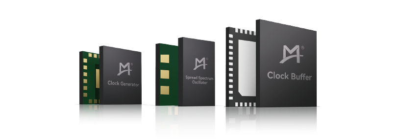
Montage Technology offers a comprehensive suite of timing solutions, including clock generators, clock buffers and spread spectrum oscillators. Widely used in data centers, communication, consumer, medical, and automotive electronics, these products address the industry's growing demand for high-performance clock chips.
With deep expertise in mixed-signal design, core IO technology, and PLL modules, Montage Technology incorporates advanced features such as high-performance PLL, low-noise IO, and high power supply rejection ratio LDO into its clock chips, delivering industry-leading performance and power efficiency. Additionally, rigorous quality control and an optimized supply chain ensure superior product reliability and long-term availability.
Core Advantages
- Proprietary technology with independent IP rights
- High performance, low power consumption
- Ultra-low phase noise
- Multiple independently configurable outputs
- Wide-ranging application scenarios
- Outstanding quality control capability
Typical Application Scenarios


Features
- Clock Generators
- Any frequency generation, compliant with PCIe® 6.0 specifications
- Independent and dynamic configuration for each clock output
- Two reference sources: on/off-chip XTAL and external clock input
- Three user-friendly control modes: I²C, OTP, and PIN
- Clock Buffers
- Up to 3.1 GHz input reference clocks, with glitch-free switchover in the TBS series
- Up to 10 differential outputs with additive RMS phase noise < 35 fs
- Independent configuration for each output bank (IO type, voltage, and enable)
- Excellent PSRR and ESD performance
- Spread Spectrum Oscillators
- Differential clock generation at any frequency from 1.22 MHz to 333.33 MHz
- Support center and down spread spectrum
- Standard 5032/3225 6-pin package
Product List
- Clock Generators
| Part Number | Input Ref Clock (MHz) | Crystal Input | # of Differential Output Clocks | LP-HCSL | HCSL | LVDS | LVCMOS | Supply Voltage (V) | Differential Output Frequency (MHz) | Package | Temperature Range (°C) |
|---|---|---|---|---|---|---|---|---|---|---|---|
| M88TG0104A | 1.22 to 250 | External, 8-50 MHz | 4 | √ | √ | √ | √ | 1.8, 2.5, 3.3 | 1 to 333.33 | 24-pin VFQFPN | -40 to +85 |
| M88TG0104B | / | Internal, 50 MHz | 4 | √ | √ | √ | √ | 1.8, 2.5, 3.3 | 1 to 333.33 | 24-pin LGA | -40 to +85 |
| M88TG0102A | 1.22 to 250 | External, 8-50 MHz | 2 | √ | √ | √ | √ | 1.8, 2.5, 3.3 | 1 to 333.33 | 16-pin LGA | -40 to +85 |
| M88TG0102B | / | Internal, 50 MHz | 2 | √ | √ | √ | √ | 1.8, 2.5, 3.3 | 1 to 333.33 | 16-pin LGA | -40 to +85 |
| M88TG0101A | 1.22 to 250 | External, 8-50 MHz | 1 | √ | √ | √ | √ | 1.8, 2.5, 3.3 | 1 to 333.33 | 12-pin LGA | -40 to +85 |
| M88TG0101B | / | Internal, 50 MHz | 1 | √ | √ | √ | √ | 1.8, 2.5, 3.3 | 1 to 333.33 | 12-pin LGA | -40 to +85 |
- Clock Buffers
| Part Number* | Max Input Ref Clock | Crystal Input (MHz) | # of Output Clock Banks | # of Diff-pair per Bank | # of LVCMOS | LVPECL | LVDS | LP-HCSL | Supply Voltage (V) | Package | Temperature Range (°C) |
|---|---|---|---|---|---|---|---|---|---|---|---|
| M88TB(S)2310A | 3.1 GHz | 8-50 | 2 | 5 | 1 | √ | √ | √ | 1.8 - 3.3 | 48-pin WQFN | -40 to +85 |
| M88TBZS2310A | 3.1 GHz | 8-50 | 2 | 5 | 1 | √ | √ | √ | 1.8 - 3.3 | 48-pin WQFN | -40 to +85 |
| M88TB(S)2308A | 3.1 GHz | 8-50 | 2 | 4 | 1 | √ | √ | √ | 1.8 - 3.3 | 40-pin WQFN | -40 to +85 |
| M88TB(S)2308H | 1 GHz | 8-50 | 2 | 4 | 1 | √ | 1.8 - 3.3 | 40-pin WQFN | -40 to +85 | ||
| M88TBZS2308A | 3.1 GHz | 8-50 | 2 | 4 | 1 | √ | √ | √ | 1.8 - 3.3 | 40-pin WQFN | -40 to +85 |
| M88TB(S)2306A | 3.1 GHz | 8-50 | 2 | 3 | 1 | √ | √ | √ | 1.8 - 3.3 | 36-pin WQFN | -40 to +85 |
| M88TB(S)2304A | 3.1 GHz | 8-50 | 2 | 2 | 1 | √ | √ | √ | 1.8 - 3.3 | 32-pin WQFN | -40 to +85 |
| M88TB(S)2304H | 1 GHz | 8-50 | 2 | 2 | 1 | √ | 1.8 - 3.3 | 32-pin WQFN | -40 to +85 | ||
| M88TB(S)1310C | 350 MHz | 8-50 | 1 | / | 10 | 1.5 - 3.3 | 32-pin WQFN | -40 to +85 | |||
| M88TB(S)2310C | 350 MHz | 8-50 | 2 | / | 10 | 1.5 - 3.3 | 32-pin WQFN | -40 to +85 | |||
| M88TB(S)2205C | 350 MHz | 8-50 | 2 | / | 5 | 1.5 - 3.3 | 24-pin WQFN | -40 to +85 | |||
| M88TB(S)2205M | 3.1 GHz | 8-50 | 2 | 2 | 5 | √ | √ | √ | 1.5 - 3.3 | 24-pin WQFN | -40 to +85 |
Note: *In the part numbers, “TBS” denotes a clock buffer with glitch-free reference switchover, “TB” denotes one without, and "TBZS" denotes a clock buffer with pin-selectable impedance of either 85Ω or 100Ω.
- Spread Spectrum Oscillators
| Part Number | Frequency Range (MHz) | Spread Mode | Pin1/2 | LP-HCSL | HCSL | LVDS | LVCMOS | Operating Voltage (V) | Package | Temperature Range (°C) |
|---|---|---|---|---|---|---|---|---|---|---|
| M88TE1D500 | 1 - 333.3 | Center, Down | OE/NC | √ | √ | √ | √ | 1.8, 2.5 | 5032 | -40 to +85 |
| M88TE1D501 | 1 - 333.3 | Center, Down | 12C | √ | √ | √ | √ | 1.8, 2.5 | 5032 | -40 to +85 |
| M88TE1D320 | 1 - 333.3 | Center, Down | OE/NC | √ | √ | √ | √ | 1.8, 2.5 | 3225 | -40 to +85 |
| M88TE1D321 | 1 - 333.3 | Center, Down | 12C | √ | √ | √ | √ | 1.8, 2.5 | 3225 | -40 to +85 |