Description
Montage Technology has launched a series of programmable clock generator chips capable of producing any output frequency between 1MHz and 333.33MHz. Leveraging Montage's advanced I/O technology, this series offers excellent jitter performance and provide a wide range of clock frequencies for low phase noise spread-spectrum applications. These chips provide 1, 2 or 4 pairs of differential clock outputs with independently configurable output characteristics. All differential clock outputs are compliant with PCIe Gen1/2/3/4/5/6 common clock and separate clock architecture specifications, meeting the high-performance requirements of existing and next-generation of PCIe devices.
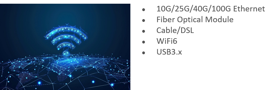
With their independently configurable clock outputs and ultra-low phase jitter performance, the devices can satisfy the demanding input reference clock needs of high-performance applications, including PCIe Gen5/6, 100G Ethernet, USB3.x, WiFi6 and more.
For more information, please contact our sales teams at globalsales@montage-tech.com.

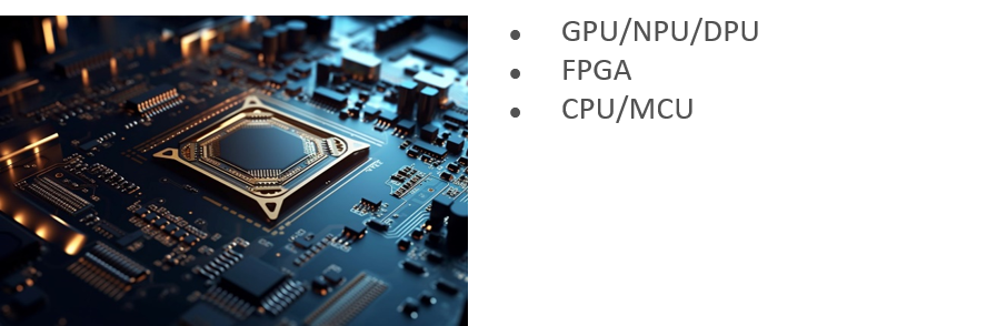
Typical Application Scenarios


Features
- 1/2/4 independently configurable clock outputs
- Output frequency: any frequency between 1MHz and 333.33MHz
- Output voltage: 1.8V/2.5V/3.3V, independent from Core voltage
- Output I/O type: LP-HCSL, HCSL, LVDS, LVCMOS
- I/O drive capability: output impedance, amplitude and enabling
- 2 spread spectrum modes (independently configurable)
- Spread spectrum mode: down, center
- Spread spectrum accuracy: 0.01%
- 3 PCIe reference clock architectures: CC, SRIS, SRnS
- 3 types of input reference clocks
- Integrated/External crystal: 8MHz to 50MHz
- External clock source: 1.2MHz to 250MHz
- 3 control modes:
- I²C Mode: support maximum 1Mb/s data rate, burst read/write mode
- OTP Mode: support dynamic switch of 4 on-chip OTP configurations
- PIN Mode: support dynamic switch of 9 SSC settings
- Low power consumption
- 2-output devices: ~ 100mW
- 4-output devices: ~ 150mW
- Working range: 1.8V to 3.3V,-40℃ to +85℃
Product List
| Part No. | Input Clock Source | Output Clock | Package |
|---|---|---|---|
| M88TG0104A | External crystal or reference clock | 4x differential clock outputs, 2x LVCMOS reference clock outputs | 4mm × 4mm × 0.75mm, 24-pin VFQFPN |
| M88TG0104B | Integrated 50MHz crystal | 4x differential clock outputs, 2x LVCMOS reference clock outputs | 4mm × 4mm × 1.10mm, 24-pin LGA |
| M88TG0102A | External crystal or reference clock | 2x differential clock outputs, 1x LVCMOS reference clock outputs | 3mm × 3mm × 1.10mm, 16-pin LGA |
| M88TG0102B | Integrated 50MHz crystal | 2x differential clock outputs, 1x LVCMOS reference clock output | 3mm × 3mm × 1.10mm, 16-pin LGA |
| M88TG0101A | External crystal or reference clock | 1x differential clock output, 1x LVCMOS reference clock output | 2.5mm × 2.5mm × 1.10mm, 12-pin LGA |
| M88TG0101B | Integrated 50MHz crystal | 1x differential clock output, 1x LVCMOS reference clock output | 2.5mm × 2.5mm × 1.10mm, 12-pin LGA |