Product Description
M88DDR4DB01 is a dual 4-bit bidirectional Gen1 DDR4 Data Buffer (DB) with differential strobes. The DB is compliant with JEDEC DDR4DB01 specification, supports data rates up to 2400MT/s and VDD supply of 1.2V. The device has a dual 4-bit host bus interface that is connected to a memory controller and a dual 4-bit DRAM interface that is connected to two x4 DRAMs. It also has an input-only control bus interface that connects to a DDR4 RCD.
All DQ inputs are pseudo-differential with an internal voltage reference. All DQ outputs are VDD-terminated drivers optimized to drive single- or dual-terminated traces in DDR4 LRDIMM applications. The differential DQS strobes are used to sample DQ inputs and are regenerated internally for driving out the DQ outputs on the opposite side of the device.
The control inputs BCOM[3:0], BCKE, and BODT are sampled by the clock inputs BCK_t and BCK_c. Additionally, M88DDR4DB01 has dedicated pins for ZQ calibration, parity check, and sequence error alerts.
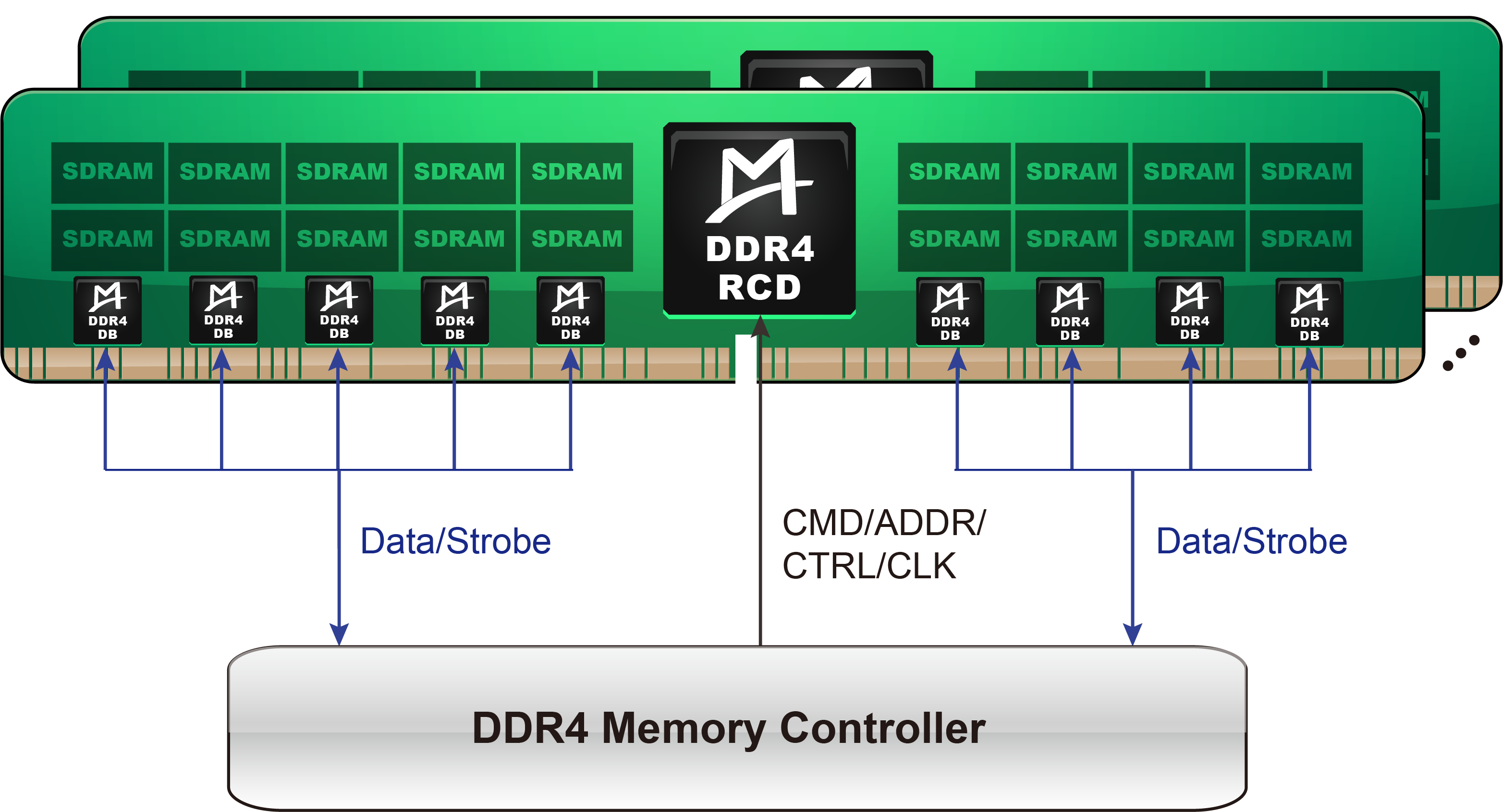
Notes: Here shows the application of DB on the DDR4 LRDIMM as an example.
Feature
- Compliant with JEDEC DDR4DB01 standard
- Speed up to DDR4-2400
- Bidirectional retiming and 1:1 redriving of DDR4 data (DQ) signals
- Regeneration of data strobe (DQS) signals from input clock
- FIFOs on the DQ path for decoupling Host and DRAM interface time domains
- Up to four package ranks supported
- Package rank timing alignment supported on the Host interface
- x4 DRAM devices supported
- Internally generated VrefDQ and independent control on Host interface and DRAM interface
- VDD voltage support: 1.2 V
- Parity error checking and sequence error checking on the BCOM interface
- DQ/MDQ input and output characteristics configurable through control registers
- Constant propagation delay from input clock to output DQ/MDQ with VT variations
- ZQ calibration of Ron and IBT values
- Synchronous ODT mode supported including a RTT_PARK feature (in addition to RTT_NOM and RTT_WR)
- Various DQ calibration support features
- Per DRAM Addressability (PDA) feature supported by transferring write data transactions from the Host interface to the DRAM interface during MRS commands issued to the DRAMs
- Per Buffer Addressability (PBA) feature supported for BCW write access commands
- Programmable write and read preamble (1tCK mode and 2tCK mode)
- Read Preamble training feature supported on the host interface
- BCW read mode and MPR read override mode supported
- No reset pin and device will enter a reset state when both BCK_t and BCK_c are LOW and BCKE is HIGH
- Input clock frequency change and dual frequency context switching supported
- Different power saving modes such as CKE low power mode, CK stop mode, etc
- Low power consumption
- Memory Bist and transparent mode supported
- Green package: Fine-pitch Ball Grid Array (FBGA)
Application
- DDR4 LRDIMM