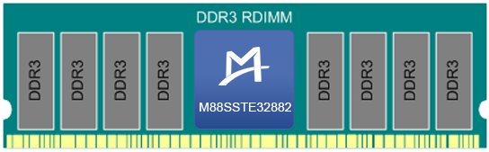
Product Description
M88SSTE32882H0 is a JEDEC-compliant Registering Clock Driver (RCD) with data rates up to 1866MT/s for DDR3/DDR3L/DDR3U RDIMM applications. The chip is 28-bit 1:2, or 26-bit 1:2 and 4-bit 1:1 configurable with parity check for address/command signals. It supports 1.5V/1.35V/1.25V VDD supply and Quad Chip Selects mode.
The device buffers the input address and control signals and redrives two copies per signal. Based on control register settings, the characteristics of the output signal can be modified to match different DIMM net topologies, while certain unused output ports can be disabled to reduce power consumption.
In addition to the functions listed in the JEDEC spec, M88SSTE32882H0 offers extra functions, including a register reading mechanism (patented) that utilizes the existing pins of the chip to monitor its internal working status, a transparent mode that helps check DRAM defects, and a dynamic frequency switching mode that helps reduce system power consumption.
Feature
- Compliant with JEDEC SSTE32882 specification
- 28-bit 1:2, or 26-bit 1:2 and 4-bit 1:1 registering buffer for DDR3 applications
- Integrated PLL clock driver distributing one differential clock pair to 4 differential pairs
- Speed up to DDR3-1866
- VDD voltage supported: 1.5 V / 1.35 V / 1.25 V
- Quad-rank DRAMs supported (quad chip selects mode)
- Parity checking on command and address signal inputs
- Output characteristics configurable through control registers
- 1T/3T MRS timing
- Pre-launch feature
- Constant propagation delay against VT variations
- Different power saving modes such as S3 low power mode, CK STOP mode, etc.
- Register read operation to monitor the chip status (patented)
- Transparent mode
- Frequency change on the fly
- Low power consumption
- Green package: 176-ball TFBGA
Application
- High-performance DDR3 RDIMM server
- High-performance computer platform