Product Description
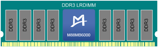
M88MB6000 is a JEDEC-compliant Memory Buffer (MB) with data rates up to 1866MT/s for DDR3 Load-Reduced DIMM (LRDIMM) applications. By buffering the command, address, control, clock and data signals of the memory channel, the chip reduces the electrical load of the memory controller and enhances the signal integrity, thus boosting the capacity and bandwidth of the memory system.
M88MB6000 supports DDR3 LRDIMMs with a maximum capacity of 64GB per DIMM, allowing the memory capacity of a single server to be increased up to 1536 GB.
Feature
- Compliant with JEDEC DDR3 Memory Buffer specification
- Speed up to DDR3-1866
- Registering and 1:2 redriving DDR3 command, address and parts of control buses
- Bidirectional retiming and 1:1 redriving of DDR3 data (DQ) signals
- Regeneration of data strobe (DQS) signals from input clock
- Generating clocks for DRAMs with a PVT stable phase relation to the input clock and redriven command, address and control signals
- Octal physical ranks supported
- x4 and x8 DRAM devices supported
- SMBus for read/write access to control registers
- On-die temperature sensor, accessible over SMBus
- Capability to supply reference voltage source for DRAMs
- Support for personality bytes
- Low power consumption
- 1.5 V, 1.35 V and 1.25 V VDD
- Green package: 588-ball FBGA
- Command/Address Processing
- Control word write procedure
- Parity checking on command/address (CA) signals
- Input bus termination (IBT) of the CA signals
- CKE power management and clock stopped power-down mode
- Dual frequency operation
- Soft CKE mode
- Refresh stagger supported
- Re-generation of ODT for DRAM interface
- Rank multiplication modes
- Address/command/control net pre-launch and post-launch
- 4 independent CKE outputs for DRAM
- 8 independent chip select (CS) outputs for DRAM
- Normal (300-1066 MHz) and test mode (70-300 MHz) frequencies
- Programmable driver characteristics for DRAM interface
- Weak drive mode of CA signals to save power
- DRAM address inversion and MRS 3T timing mode
- Data Processing
- One bidirectional data and data strobe DRAM interface
- One bidirectional data and data strobe memory controller interface
- 72 data and 18 differential data strobe signals
- FIFOs for decoupling controller and DRAM interface time domains
- Two timing modes for controller interface: minimum latency and minimum skew
- Standard DDR3 DRAM requirements for the controller interface I/Os
- Optimized low power I/Os for the DRAM interface
- Write leveling support for the controller interface
- On-chip calibration engine for DRAM interface read/write leveling and DQ/DQS relation
- DFx Features
- Transparent mode
- Memory BIST
- Voltage margin test
- Error injection
Application
- High-performance DDR3 servers
- Workstations
- Storage systems
- Networking equipment
- High-end desktop computers