
 Memory Interconnect
 PCIe® Interconnect
 CXL® Interconnect





 Contact Us


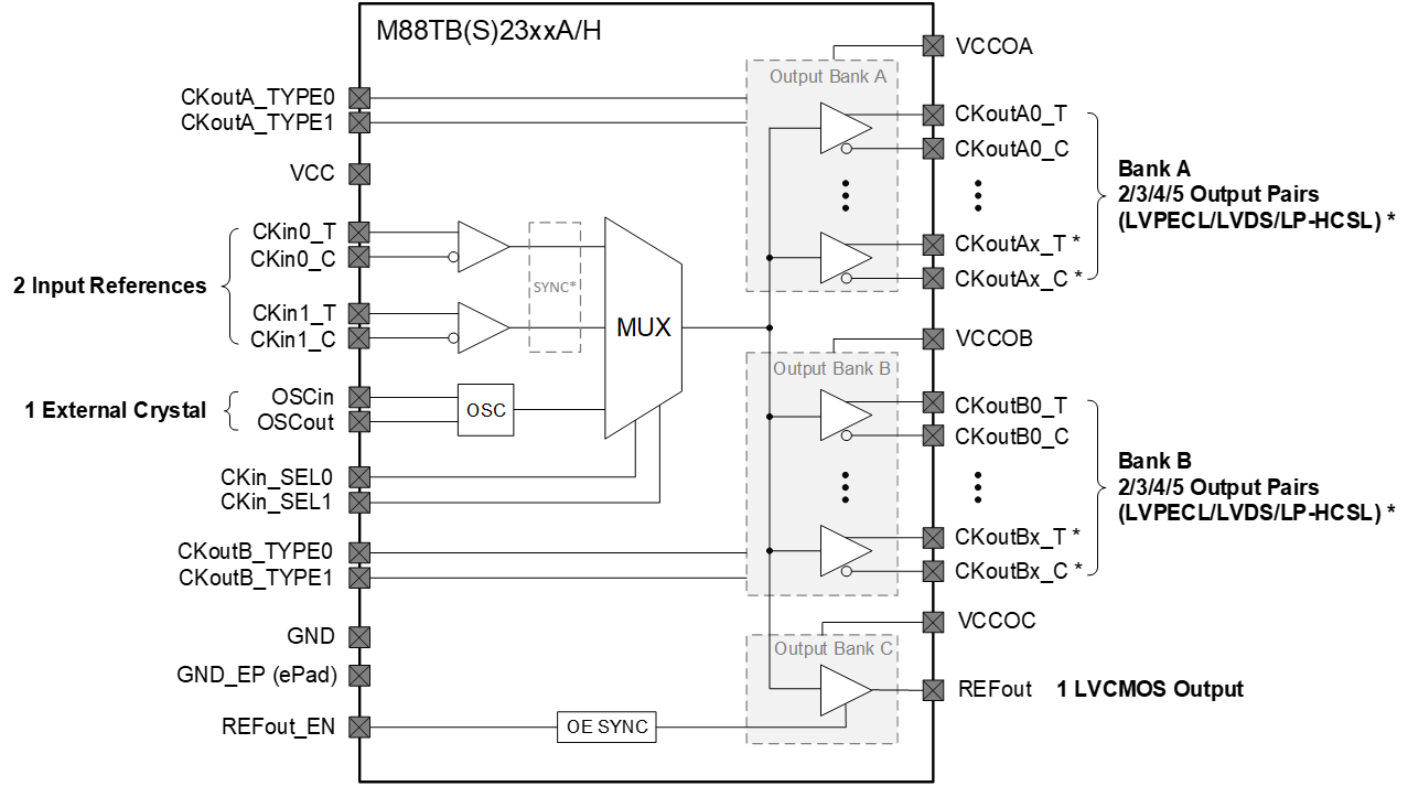
M88TB(S)23xxA/H Block Diagram
General Clock Buffer
Montage Technology’s M88TB(S)xxxxx series is a portfolio of general-purpose clock buffers that provide stable and reliable clock signals for applications in communications, industrial control, consumer electronics, and embedded systems. Comprising 22 device models, the series can be paired with Montage Clock Generators to provide customers with a comprehensive, one-stop clock tree solution.
Features
-
 Ultra-low additive jitter, as low as 35 fs (typ.) @ 156.25 MHz
-
Supports 2 to 3 reference clock inputs with input frequencies up to 3.1 GHz
-
Supports asynchronous or synchronous glitch-free clock switching
-
Supports up to 10 outputs with configurable output types, including LVPECL, LVDS, LVCMOS, LP-HCSL, and HCSL
-
Supports 1.5 V to 3.3 V operating voltage range, with independent power supply rails
-
Excellent PSRR and enhanced ESD protection
Product List
|
Part No*
|
Max Input
Ref Clock  |
Crystal Input
(MHz) |
Diff. Clock
Output (#) |
Diff Output Type
|
LVCMOS
Output (#) |
Supply Voltage
(V) |
Package
|
Temp. (°C)
|
Document
|
|---|---|---|---|---|---|---|---|---|---|
| M88TB(S)2310A | 3.1GHz | 8-50 | 10 (2 banks x 5) | LVPECL, LVDS, LP-HCSL | 1 | 1.8-3.3 | 48-pin WQFN | -40 to +85 | Product Brief |
| M88TBZS2310A | 3.1GHz | 8-50 | 10 (2 banks x 5) | LVPECL, LVDS, LP-HCSL | 1 | 1.8-3.3 | 48-pin WQFN | -40 to +85 | Product Brief |
| M88TB(S)2308A | 3.1GHz | 8-50 | 8 (2 banks x 4) | LVPECL, LVDS, LP-HCSL | 1 | 1.8-3.3 | 40-pin WQFN | -40 to +85 | Product Brief |
| M88TB(S)2308H | 1GHz | 8-50 | 8 (2 banks x 4) | LP-HCSL | 1 | 1.8-3.3 | 40-pin WQFN | -40 to +85 | Product Brief |
| M88TBZS2308A | 3.1GHz | 8-50 | 8 (2 banks x 4) | LVPECL, LVDS, LP-HCSL | 1 | 1.8-3.3 | 40-pin WQFN | -40 to +85 | Product Brief |
| M88TB(S)2306A | 3.1GHz | 8-50 | 6 (2 banks x 3) | LVPECL, LVDS, LP-HCSL | 1 | 1.8-3.3 | 36-pin WQFN | -40 to +85 | Product Brief |
| M88TB(S)2304A | 3.1GHz | 8-50 | 4 (2 banks x 2) | LVPECL, LVDS, LP-HCSL | 1 | 1.8-3.3 | 32-pin WQFN | -40 to +85 | Product Brief |
| M88TB(S)2304H | 1GHz | 8-50 | 4 (2 banks x 2) | LP-HCSL | 1 | 1.8-3.3 | 32-pin WQFN | -40 to +85 | Product Brief |
| M88TB(S)1310C | 350MHz | 8-50 | / | / | 10 (1 bank x 10) | 1.5-3.3 | 32-pin WQFN | -40 to +85 | Product Brief |
| M88TB(S)2310C | 350MHz | 8-50 | / | / | 10 (2 banks x 5) | 1.5-3.3 | 32-pin WQFN | -40 to +85 | Product Brief |
| M88TB(S)2205C | 350MHz | 8-50 | / | / | 5 (2 banks: 2 + 3) | 1.5-3.3 | 24-pin WQFN | -40 to +85 | Product Brief |
| M88TB(S)2205M | 3.1GHz | 8-50 | 2 (1 bank x 2) | LVPECL, LVDS, LP-HCSL | 3 (1 bank x 3) | 1.5-3.3 | 24-pin WQFN | -40 to +85 | Product Brief |
Note: *In the part numbers, “TBS” denotes a clock buffer with glitch-free reference switchover, “TB” denotes one without, and "TBZS" denotes a clock buffer with pin-selectable impedance of either 85Ω or 100Ω.


Applications
PCIe Gen1 - Gen7 and NVLink
Reference clocks for ADCs, DACs, RF transceivers, SATA/SAS, and Ethernet
Data center servers, switches, storage systems, and other equipment
Communications equipment, including wireless base station BBU/RRU, core network routers, switches, and PON
For product details, please contact us.
